1.Build a circuit with no inputs and one output. That output should always drive 1 (or logic high).
建立一个没有输入和一个输出的电路。该输出应始终驱动 1(或逻辑高)。
题目:
module top_module( output one );

// Insert your code here

    assign one = [fixme];

endmodule
解答:
module top_module( output one );

// Insert your code here

    assign one = 1'b1;

endmodule
结果:success!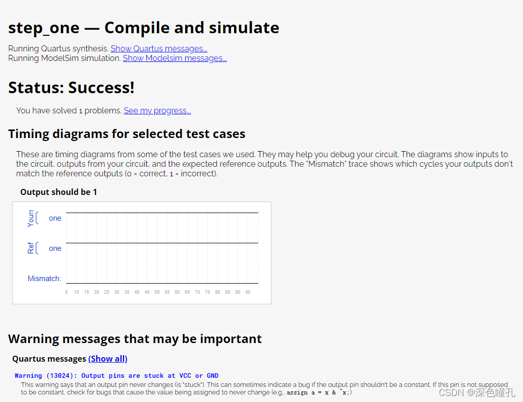
那么逻辑低电是什么那?详情啊见评论
2.Build a circuit with no inputs and one output that outputs a constant 0
建立一个没有输入和一个输出的电路,输出一个常数0
题目:
module top_module(
    output zero
);// Module body starts after semicolon

endmodule
解答:
module top_module(
    output zero
);// Module body starts after semicolon
    assign zero=1'b0;
endmodule
结果: 尴尬了,这里输入assign one=1’b0 结果出错,哈哈哈哈哈哈,看准题目要求,不要硬搬硬套
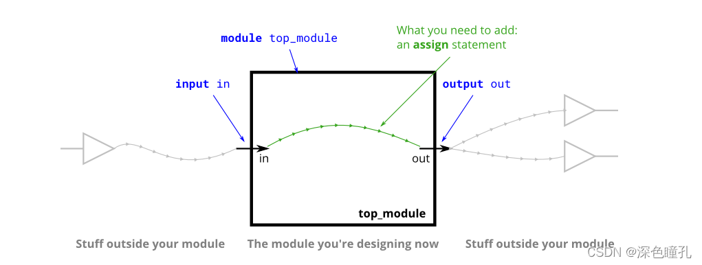
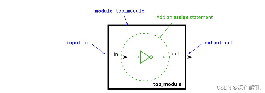
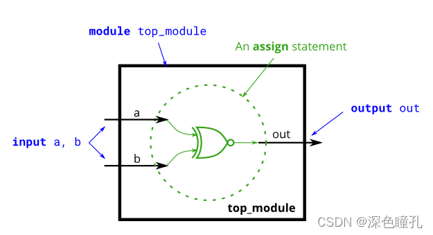
The diagram below illustrates how each part of the circuit corresponds to each bit of Verilog code. The module and port declarations create the black portions of the circuit. Your task is to create a wire (in green) by adding an assign statement to connect in to out. The parts outside the box are not your concern, but you should know that your circuit is tested by connecting signals from our test harness to the ports on your top_module.
下面的图表说明了电路的每一部分如何对应于 Verilog 代码的每一位。模块和端口声明创建电路的黑色部分。您的任务是通过添加要连接 in to out 的 assign 语句来创建连接(绿色)。盒子外面的部件与你无关,但是你应该知道你的电路是通过连接信号从我们的测试线束测试到你的顶部模块的端口。
问题:
module top_module( input in, output out );

endmodule
解答:
module top_module( input in, output out );
  assign out=in;
endmodule
结果: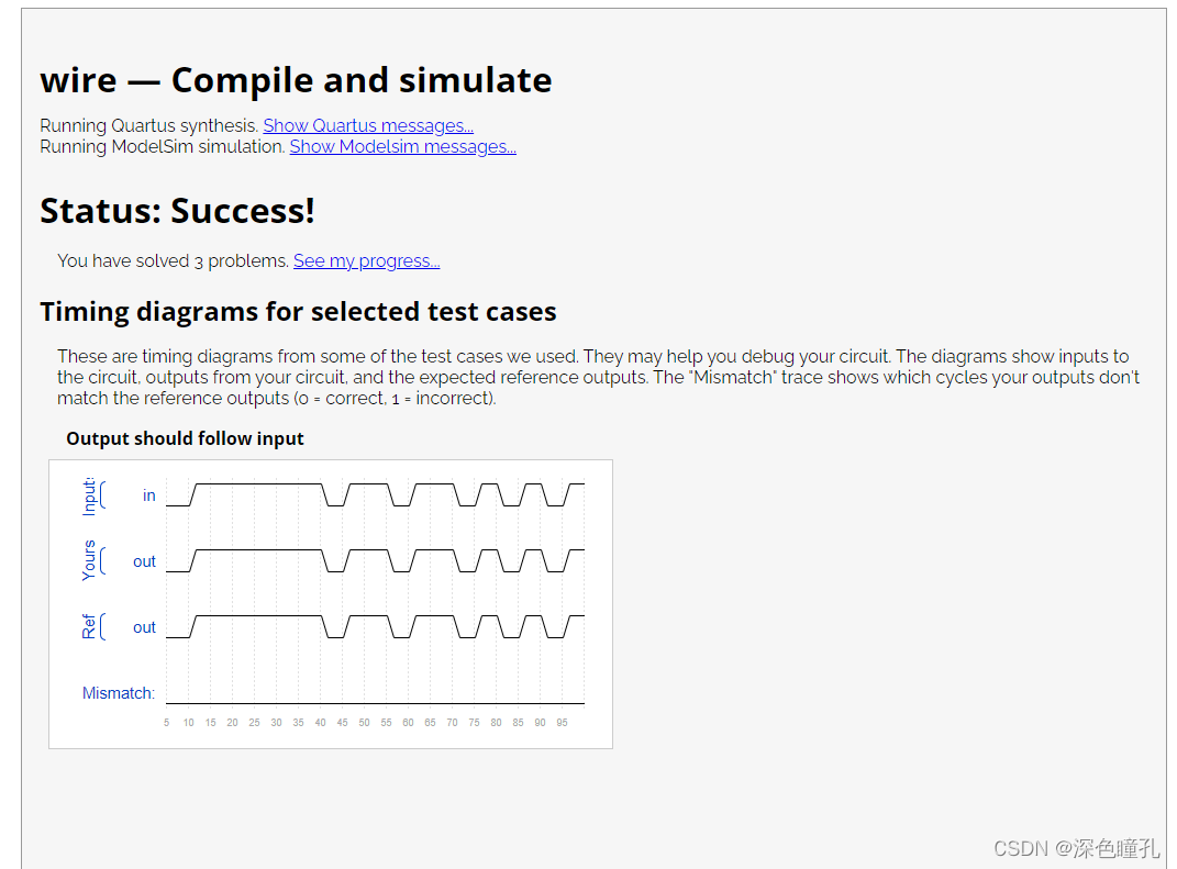
4.Create a module with 3 inputs and 4 outputs that behaves like wires that makes these connections:
a -> w
b -> x
b -> y
c -> z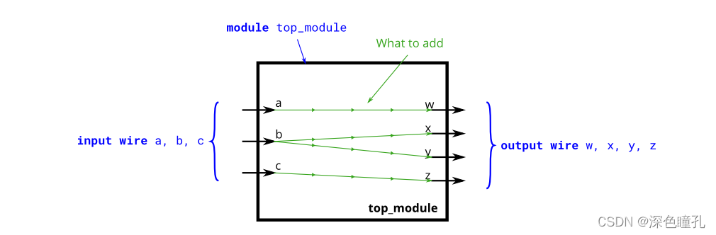
解答:
module top_module(
    input a,b,c,
    output w,x,y,z );
	assign w=a,z=c,x=b,y=b;
endmodule
结果: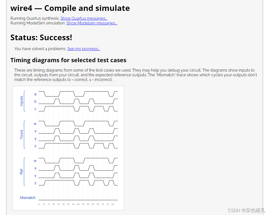
5.Create a module that implements a NOT gate.
解答:
module top_module( input in, output out );
	assign out=~in;
endmodule
结果: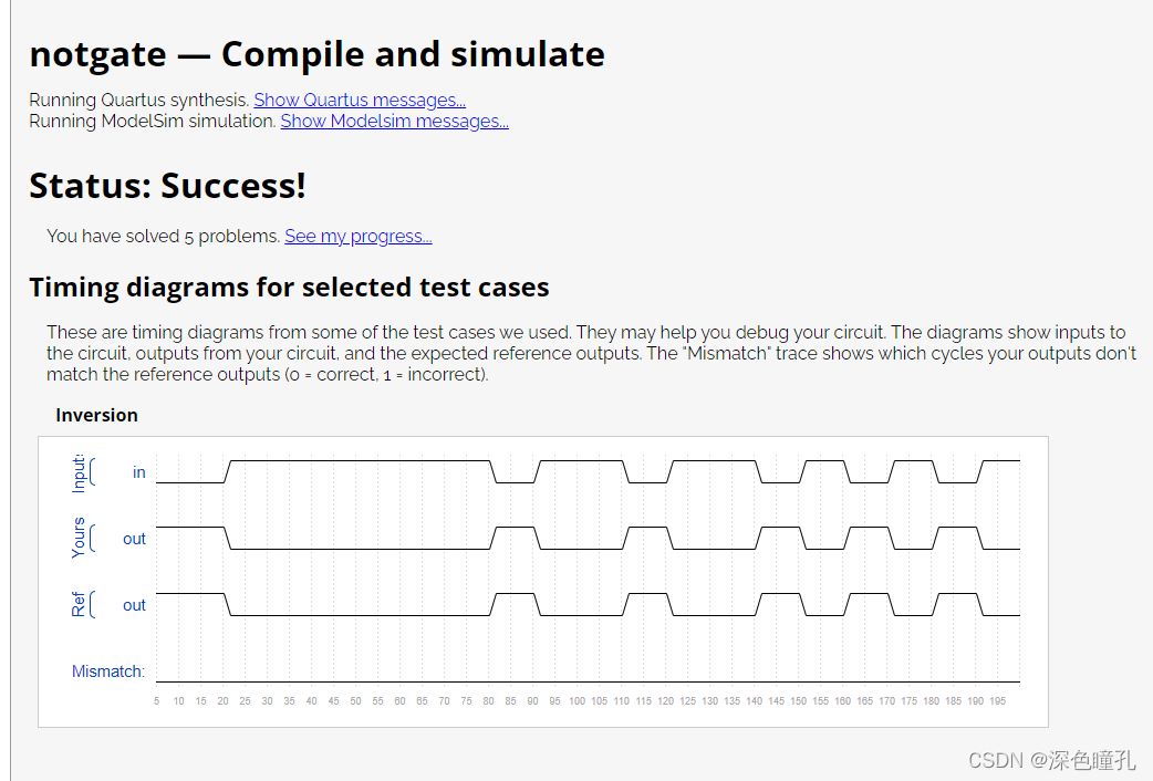
问题来了,为什么是~符号不是!符号
下面这个是将~改为!,仍然正常输出结果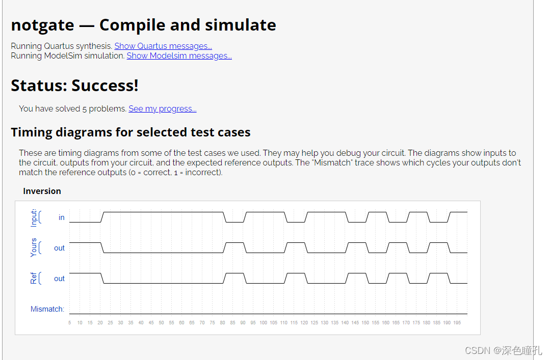
区别:
按位运算符进行逐位的逻辑运算(如:与或非),输出与输入位数一致;
逻辑运算符进行逻辑运算,不关注输入的某一位而是将输入作为整体进行逻辑操作,输出位数为1;
列举:
与:& 按位与;&& 逻辑与;
或:| 按位或;|| 逻辑或;
非:~ 按位非;! 逻辑非;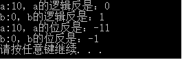
缩位运算符:
灵活使用缩位运算符,可以简化代码,避免重复工作;
如:
 &a  可实现a各位间的与运算,即:&a等价于 a(0)&a(1)&...&a(n)

 | a  可实现a各位间的或运算,即:| a等价于 a(0)|a(1)|...|a(n)
{}迭代连接运算符:
连接功能:将若干个寄存器类型/线网类型的变量首尾连接,形成一个更大位宽的变量;
如:
    a = 2'b10;

    b = 3'b010;

   有{a,b} = 5'b10010;
迭代功能:把一个变量复制多次,首尾连接组成一个更大位宽的变量;(实际仍为连接功能的一个特例:连接元素相同)
如:

    a = 2'b10;

   有{4{a}},即{a,a,a,a}
注意:
要保证迭代的完整性:{ {4{a}},b}   ({4{a}}为迭代功能,括号不能少;即不能写为{ 4{a},b} )
迭代连接运算符还可用于常量操作:{ {4{1'b1}},2'b10}
Verilog逻辑移位运算符与数字移位运算符:
列举:
    << 逻辑左移运算符;<<< 数字左移运算符;
    >> 逻辑右移运算符;>>> 数字右移运算符;
区别:
逻辑移位运算符不关心符号位;逻辑左移右端补零,逻辑右移左端补零;
数字左移位运算符不关心符号位,与逻辑左移一样;数字右移运算符关心符号位,左端补符号位;
如:
    1010101010,其中[]是添加的位

    逻辑左移一位:010101010[0]

    算数左移一位:010101010[0]

    逻辑右移一位:[0]101010101

    算数右移一位:[1]101010101
进行部分仿真(感觉很简单,着手去编写的时候却碰见了不少问题,万不可眼高手低!!!)
6.Create a module that implements an AND gate.
 解答:
解答:
module top_module(
    input a,
    input b,
    output out );
	assign out=a&b;
endmodule
结果: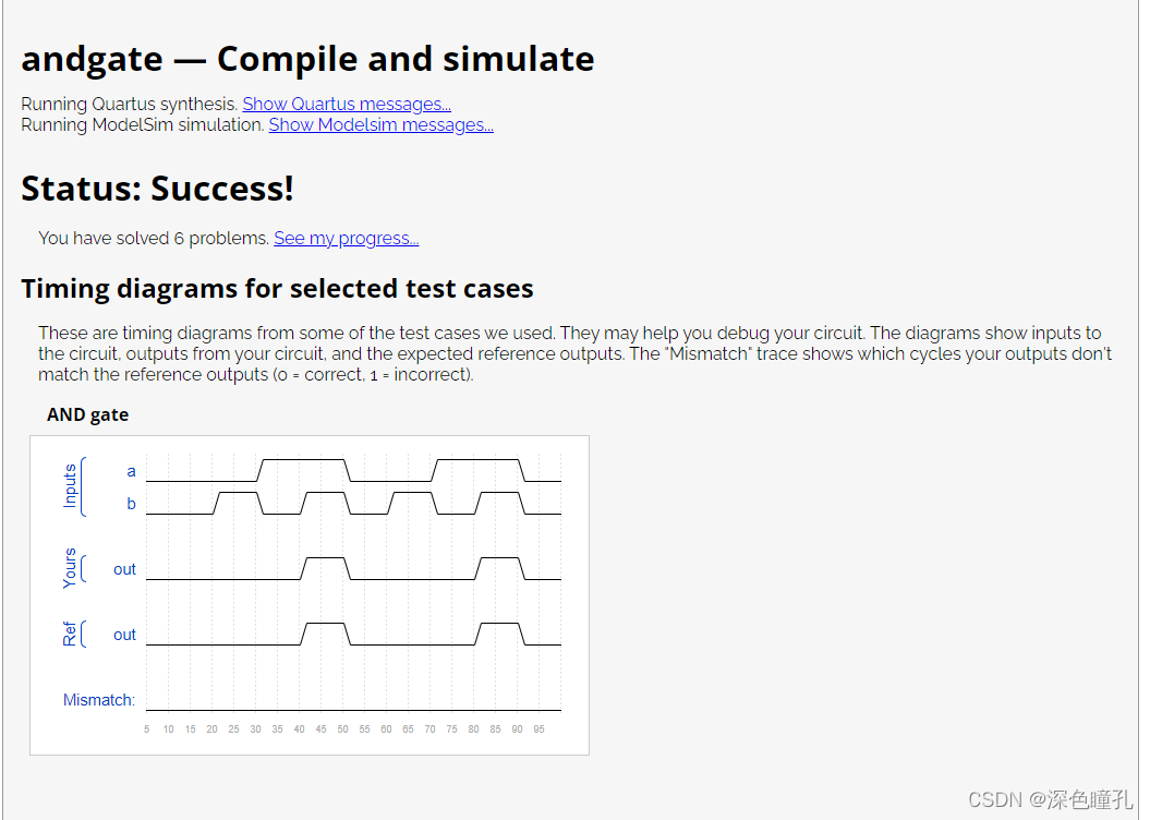
同理 & 和 && 也是分为逻辑and和位and
7.Create a module that implements a NOR gate. A NOR gate is an OR gate with its output inverted. A NOR function needs two operators when written in Verilog.
创建一个实现NOR门的模块。NOR门是输出反向的或门。在Verilog中编写NOR函数时需要两个操作符。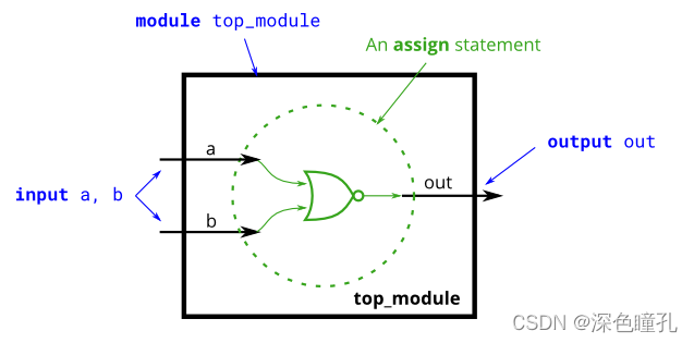
解答:
module top_module(
    input a,
    input b,
    output out );
    assign out=!(a&b);
endmodule
结果: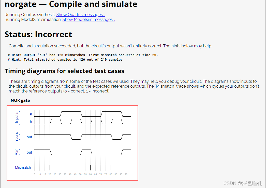
有点小问题呀
改成了~也不对哈哈哈
正确解答:
module top_module(
    input a,
    input b,
    output out );
    assign out=!(a|b);
endmodule
贼贼,看错了不是,哈哈哈哈是或不是与呀,同时在这里还解答了我的一个疑问
使用逻辑还是按位!
题目中的Hint:Verilog has separate bitwise-OR (|) and logical-OR (||) operators, like C. Since we’re working with a one-bit here, it doesn’t matter which we choose.
So,it doesn’t matter!
正确结果: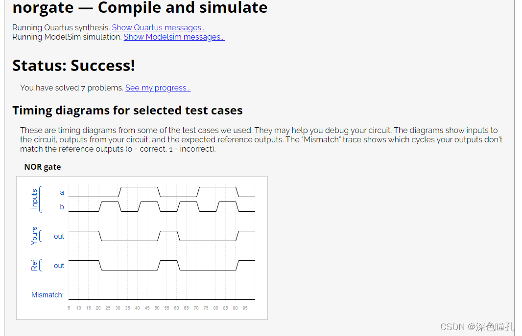
8.Create a module that implements an XNOR gate.
解答:
module top_module(
    input a,
    input b,
    output out );
    assign out=!(a^b);
endmodule
结果: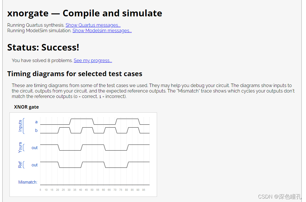
一次成功,一个小小的异或门[狗头]
这个Verilog操作符(逻辑操作符,位操作符,递减操作符Reduction Operators),异或运算
可以看这个博客:Verilog操作https://blog.csdn.net/llxxyy507/article/details/82223296?,改天我也总结一篇
9.Declaring wires
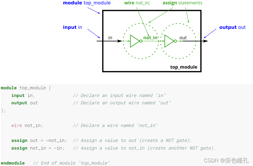
The circuits so far have been simple enough that the outputs are simple functions of the inputs. As circuits become more complex, you will need wires to connect internal components together. When you need to use a wire, you should declare it in the body of the module, somewhere before it is first used. (In the future, you will encounter more types of signals and variables that are also declared the same way, but for now, we’ll start with a signal of type wire).
Example
题目:
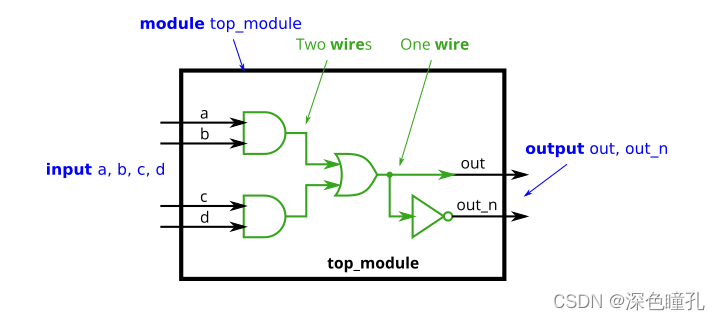
解答:
`default_nettype none
module top_module(
    input a,
    input b,
    input c,
    input d,
    output out,
    output out_n   );

    wire pr_out1,pr_out2,se_out;
    assign out=se_out,out_n=~se_out;
    assign se_out=pr_out1|pr_out2;
    assign pr_out1=a&b,pr_out2=c&d;
endmodule
10.7458
The 7458 is a chip with four AND gates and two OR gates. This problem is slightly more complex than 7420.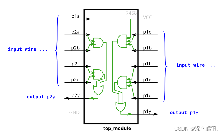
解答:
module top_module (
    input p1a, p1b, p1c, p1d, p1e, p1f,
    output p1y,
    input p2a, p2b, p2c, p2d,
    output p2y );
	wire p2_af1,p2_af2,p1_af1,p1_af2;
    assign p2_af1=p2a&p2b,p2_af2=p2c&p2d;
    assign p2y=p2_af1|p2_af2;
    assign p1_af1=p1a&p1b&p1c,p1_af2=p1d&p1e&p1f;
    assign p1y=p1_af1|p1_af2;

endmodule
结果: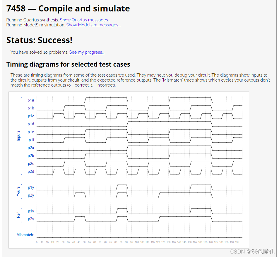
仍需努力,加油加油加油~