Introduction
logic gate are the basis of a computer hardware. Without the invention of logic gate, computers can't be designed... not even any electronic devices. A logic gate only produces one output but can have multiple inputs. It processes the input boolean value(s) by a logical operation such as AND, OR, NOT, XOR and so on.
Be careful! Boolean circuit wise, when we say "give an value", it means that the logic gate produces a TRUE value. Because logic True and logic False are physically represented by voltage - no or low voltage is False (0), and high voltage indicates True (1). So give an value means "high voltage".
In the article, we will use 1s / 0s, high / low voltage, and give an value / not give an value interchangeably. Also, the website that we use to show logic gate is: Logic.ly https://logic.ly/demo/ you can have a play with it.
basic gates
AND gate
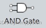
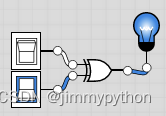
what is logic AND? It gives an value only when both inputs are true, which means that only for input 1, 1 it produces 1. For example, you say: I own a extravagent mansion AND I am paid 100,000 pounds annually. So only when both conditions are satisfied, you statement is true.
OR gate

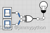
waht is logic OR? the logic gate produces 1 when at least one of the two (multiple) inputs is true, which means that for 0,1 or 1,0 or 1,1, the gate will produce a true value. For example, you tell a fairy: I want a high salary or a big house. She only needs to realise at least one of your wishes.
NOT gate

A NOT gate is very simple. for any value inputed, the gate gives the reversed output. For example you input 0 it outputs 1.
XOR gate
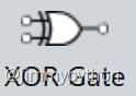
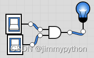
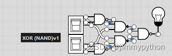
XOR stands for "excluded OR". It returns a value when either of the inputs is true. It can be represented by a combination of logic gates.
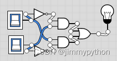
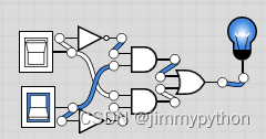
The combinational logic gate shown above simulates the functionality of a XOR gate. Some people may find it plausibly complicated. Later on we will devise how these combinational ones are devised.
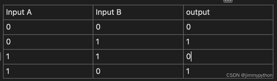
Truth table
Truth table is simply a table that enumerates all possible input combinations and the according output under the law of a basic/combinational logic gate.
truth table are usually used to build logic gate. How?
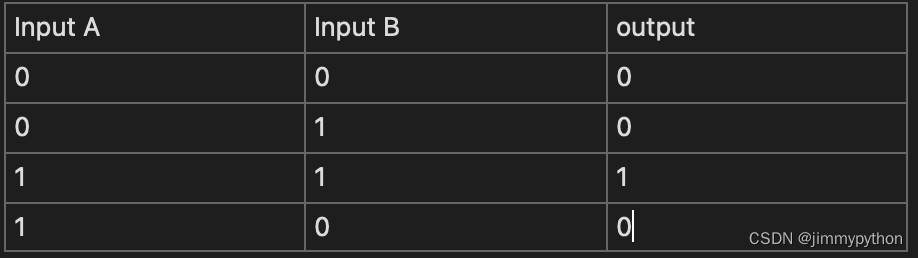
Inputs and intended output are entered for all possible values. We want to find all possible rows of inputs that make the output true. For example, in the truth table for XOR gate, we can see that the output will be true when input A is 0, B is 1, or when input A is 1, B is 0.
In the two valid pairs of inputs, we need to identify the input that is 0 and turn it to 1 by not gate, and use AND gate to connect the two inputs. For example, in the second row of the truth table of XOR gate, the input A is 0 while the input B is 1, then we do: !A*B; similarly, for the last row, we have A*!B.
Two possible combinations of inputs both produce an output of 1, so we use OR gate to connect these two -- then we have the expression for XOR gate by OR, AND, and NOT gate: !A*B+A*!B.
However, usually, this is not the last step. Some more complicated boolean expressions can be simplified. We simplify it because we want to use as few gates as possible to achieve the function for cost-effectiveness.
Boolean Algebra
A AND B is represented as A*B, or A∧B, A&B which is logic multiplication. This makes sense in set operation...
A OR B is A+B, A∨B, A|B which is logic addition
NOT A is usually represented as ¬A, Ā, 'A, !A
A XOR B is: A⊕B, A⊻B, A^B
similar to number operation, we do have some rules of arithmetics in boolean operation
general rules
A*0=0, A*1=1, A*A=A, A*~A=0
A+1=1, A+0=A, A+A=A, A+~A=1
A*B=B*A, A+B=B+A (commutative rules)
A+B+C=A+(B+C), A*B*C=A*(B*C) (associative rules)
A*(B+C)=A*B+A+C, A+(B*C)=(A+B)*(A+C) (distributive rules)
A+(A*B)=A, A*(A+B)=A (absorption rules) (proof: try (A*1)+(A*B) , the second equation can be transformed to the first)
~(A*B)=~A+~B, ~(A+B)=~A*~B (De Morgan) (can be proved via Venn diagram)
A=~~A (double negative)
Use the powerful internet if you want to prove some of them.
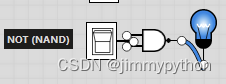
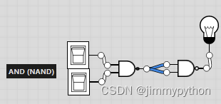
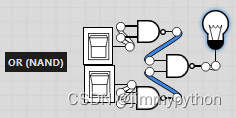
NAND gate
why do we sometimes use a combination of logic gates to represent another basic logic gate?
Mass production of a circuit is cheaper than producing all in a small amount. If we use one circuit to represent others, we save cost. However, in some circumstances, representing a circuit by a combination of logic circuit would become too unnecessarily complicated, and the efficiency decreases.
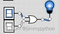
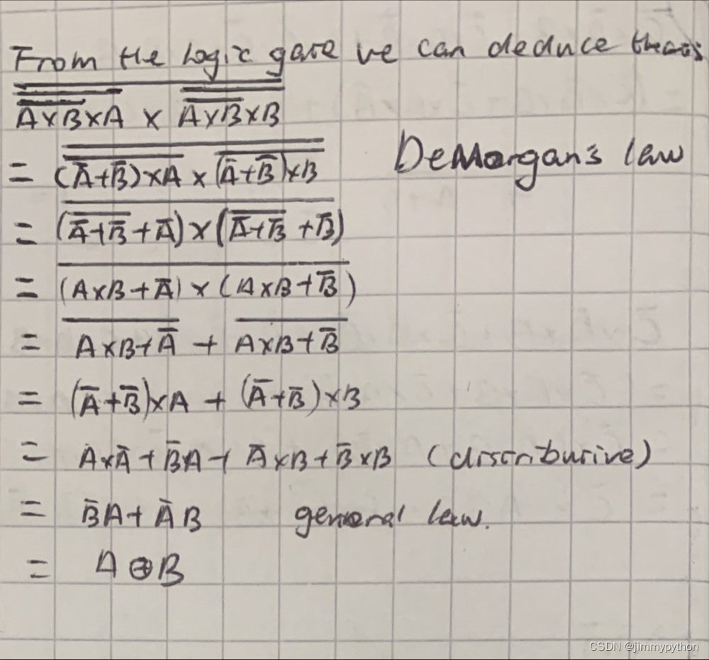
nand gate is the AND gate followed by a NOT gate. It is said that NAND gate can represent all the basic circuits.
Use NAND gate to represent all the basic gates. How do we figure out why they make sense? use boolean algebra to prove it. Dont worry, it's quite easy!
XOR
This is purely obtained from the boolean expression, by the truth table.
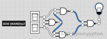
Notice that this one achieve the function with one less gate! this can be proved to function using boolean algebra. We firstly look at the gate above and use all possible combinations of inputs and correspond outputs to produce a truth table. From the table we can get a boolean expression. Then we simplify it and found that it equals !A*B+A*!B.
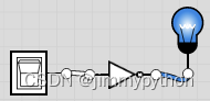
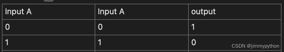
NOT
AND
OR
to prove this, we use De Morgan's law: !A*!B=!(A+B)
then: !(!A*!B)=!(!(A+B))
then: !(!A*!B)=A+B (double negative)
Useful circuits
half adder and full adder
The full adder is the combinational logic gate that enables the computer to calculate binary numbers physically.
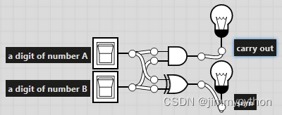
half adder
Half adder is a simplified version of a full adder. This is a machine that add one digit of one binary with another. How does it do addtion?
Assume that all of you have learnt about binary arithmetics.
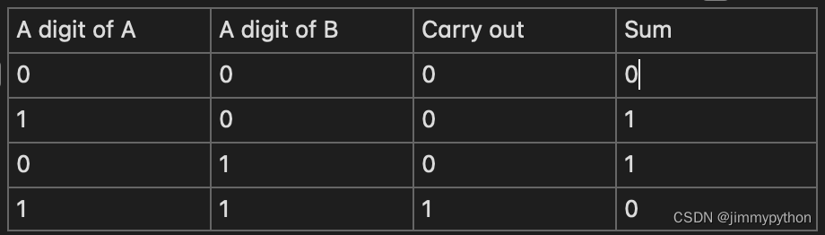
I made a truth table that takes all possible combinations of inputs and produces intended outputs.
now we make a boolean expression that relates the digit of A and the digit of B to the output: A*!B + !A*B->Sum, A*B->Carry out. The first expression can be simplified to A⊕B. So, we make logic gates base on these expressions!
Full adder
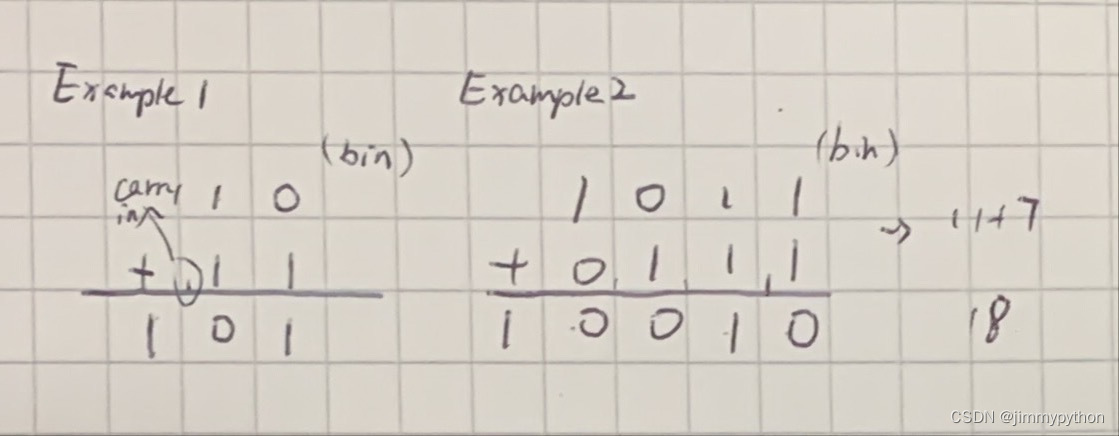
What if we want to calculate several digits? for example 10+11 (bin)? Then we need to consider the carry in.
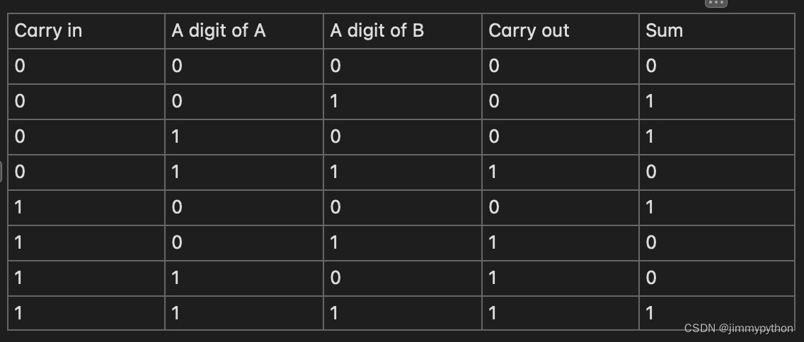
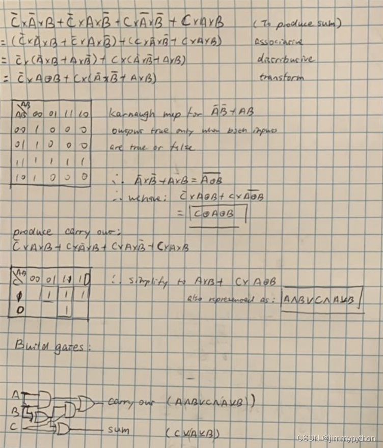
The truth table above shows all useful combinations of three inputs and according outputs. We makes boolean expressions out of it and simplified it as usual. Note carry in as C. For Sum, we have: !C*!A*B+!C*A*!B+C*!A*!B+C*A*B. For carry out, we have: !C*A*B+C*!A*B+C*A*!B+C*A*B
This is wayyyyy too complicated, if a firm designs full adders using the expressions provided above, it will bankrupt immdiately. If it doesn't bankrupt, consumers suffer - opening a web page may need several minutes and the game design will be impractical because it's too slow.
so we need to simplify the boolean expressoin above!
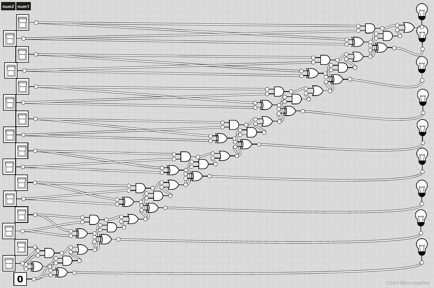
that's a one digit full adder. Usually, we use much bigger full adders with several bytes. I am going to show you a 8-digit full adder.
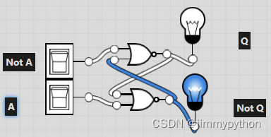
D-latch
J-latch
The purpose of this D-latch is to store data when there is no current (input)
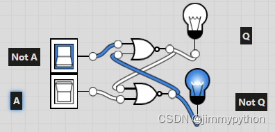
If you enter an input, it gives an ouput which will hold on even if the input is turned off
D-latch A-level version
Registers need to store different data temporarily and release them regularly following the clock speed. So we need to add a clock into this model so it's change in output responses to the input and the clock.
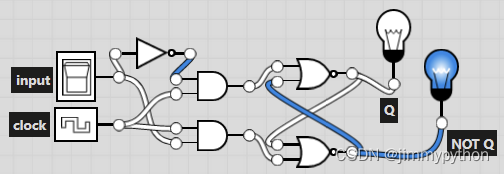
it is said that this is only a simplified version of a D-latch.